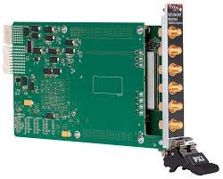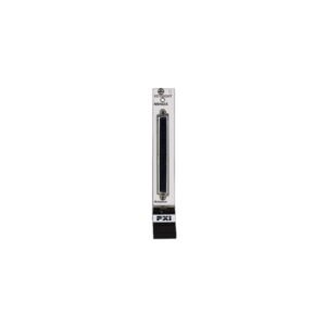

The NI PXI-7842 and PXI-7842R are R-Series PXI Multifunction Reconfigurable I/O Modules built for high-speed, adaptable I/O in demanding test and control environments. Each module integrates a user-programmable FPGA—Xilinx Kintex-7 for the PXI-7842R or Artix-7 for the PXI-7842—enabling custom control logic and onboard signal processing. With 80 digital I/O channels, 16 analog inputs, and 8 analog outputs, plus direct memory access (DMA) to FPGA and host, these modules excel at real-time data acquisition, hardware-in-the-loop (HIL) testing, and custom instrumentation within PXI systems.
Technical Specifications
FPGA & Memory
• Xilinx Kintex-7 FPGA (PXI-7842R); Xilinx Artix-7 FPGA (PXI-7842)
• DDR3 SDRAM: 1 GB (PXI-7842R), 512 MB (PXI-7842)
Digital I/O
• 80 channels across 32 banks of 8 channels
• Individually configurable per bank for input or output
• Voltage levels: 1.2 V, 1.8 V, 2.5 V, 3.3 V, 5 V (software-selectable)
• Update rate: Up to 100 MS/s single-point I/O
• Programmable input thresholds per channel or bank
• Open-drain outputs supported
• DMA access to FPGA and host memory
Analog Input
• 16 channels, 16-bit resolution
• Simultaneous sampling at up to 2 MS/s per channel
• Input ranges: ±10 V, ±5 V, ±1 V, ±0.2 V (software-selectable)
• DC coupling; input impedance 1 MΩ || 20 pF (typ.)
• 10 kHz bandwidth analog antialiasing filter
• AC coupling available through FPGA programming
Analog Output
• 8 channels, 16-bit resolution
• Update rate: Up to 1 MS/s per channel
• Output ranges: ±10 V, ±5 V, ±1 V (software-selectable)
• Output current: ±5 mA (typ.); output impedance < 10 Ω (typ.)
• Configurable minimum dwell time via FPGA
Clocking & Synchronization
• Onboard high-precision clock for deterministic operation
• External TTL-compatible clock input
• PXI trigger line support (0-7)
• Programmable FPGA clocking for custom timing
Connectivity
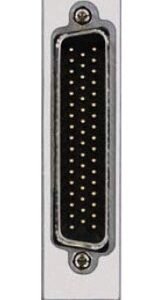
• 1 × 100-pin SCB-100 or shielded digital I/O connector
– Key Features
• Field-programmable FPGA for custom logic and signal processing
• Multi-voltage digital I/O reduces interface complexity
• Simultaneous analog input sampling enables phase-coherent measurements
• Direct DMA path minimizes latency in data streaming
• Programmable input thresholds and open-drain outputs support mixed-signal applications
– Typical Applications
• Real-time data acquisition systems
• Hardware-in-the-loop (HIL) simulation and testing
• Custom instrumentation and signal conditioning
• Synchronous multi-channel measurement and control
– Compatibility & Integration
Both modules integrate into PXI chassis and leverage the PXI trigger infrastructure for system-level synchronization. FPGA reconfigurability enables adaptation to specific measurement, control, and signal-processing requirements without redesign.