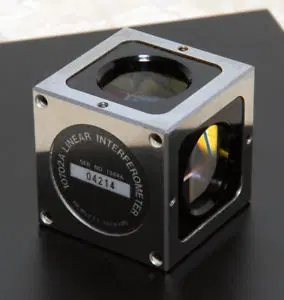

The Spex / Horiba LEM-P-CC-R-C is a Camera Endpoint Monitor that employs real-time laser interferometry for precision detection of film thickness and trench depth during etching and deposition processes. The system mounts directly above the wafer to capture interference patterns generated when monochromatic laser light interacts with sample surfaces. This enables continuous monitoring of etch/deposition rates, thickness variations, and layer interfaces with a laser spot diameter ranging from 20 µm to 100 µm. The LEM-P-CC-R-C integrates into dry etch/deposition chambers and supports multiple laser wavelengths across visible and near-infrared bands, making it compatible with diverse film materials and process windows.
Technical Specifications
• Measurement Technique: Real-time laser interferometry
• Laser Wavelengths: 670 nm (visible), 808 nm, 905 nm, 980 nm (near-infrared)
• Laser Spot Diameter: 20 µm to 100 µm
• Objective Lens to Wafer Distance: 200 mm to 800 mm
• Image Capture: Real-time digital CCD imaging
• Illumination: Adjustable intensity control for varying sample reflectivity
– Key Features
• Configurable as standalone sensor (LEM Sensor) with analog output or complete instrument (LEM-CT) with Sigma_P software control
• XY stage options: manual, motorized, or motorized with controller and joystick
• Manual and optional motorized tilt functions for perpendicularity adjustment
• LEM-CT offers TCP/IP and RS 232 remote connectivity; supports SECS, HSMS, Fab LAN protocols
• Requires measurement viewport of ø20 mm or greater
– Typical Applications
• Etch and deposition rate monitoring
• Endpoint detection for multi-layer film processes
• Film thickness and trench depth measurement
• Interface detection and fringe counting
– Compatibility & Integration
Supports SiN, SiO2, GaAs, InP, AlGaAs, and GaN films. Mounts on any process chamber with direct top-view wafer access. Suitable for OEM integration and process development in industrial R&D environments.