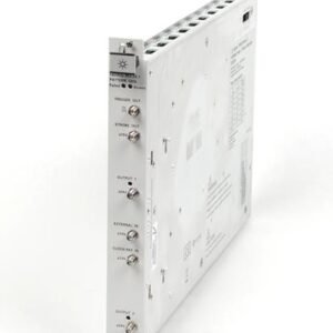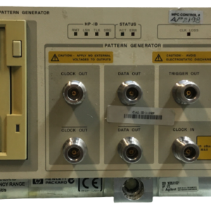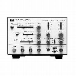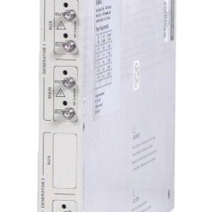

The Tektronix DG2030 is a digital data pattern generator engineered for precise signal generation across digital communication systems, semiconductor characterization, and logic circuit testing. With a frequency range of 0.1 Hz to 409.6 MHz and data rates up to 409.6 Mbps, this instrument delivers four standard channels (expandable to eight) with 256 K word pattern memory and a 4000-step sequence controller. The DG2030 excels at timing margin analysis, setup and hold violation simulation, and metastability condition generation—critical for device and circuit evaluation where amplitude and timing precision determines test validity.
Technical Specifications
Signal Generation
• Frequency Range: 0.1 Hz to 409.6 MHz
• Data Rate: Up to 409.6 Mbps
• Channels: 4 standard; expandable to 8 with Option 01
• Pattern Memory: 256 K word per channel
• Pattern Depth: 90 to 256 Kbits per channel
• Sequence Controller: 4000-step with external trigger capability
Output Characteristics
• Output Voltage (into 50 Ω): VOH −1.25 V to +3.5 V; VOL −1.50 V to +3.25 V
• Programmable Range: −1.5 V to +3.5 V
• Output Swing: 250 mVp-p to 5 Vp-p
• Output Impedance: 50 Ω
• Voltage Resolution: 5 mV
• DC Accuracy: ±3% of setting ± 50 mV
• Signal Aberrations: ≤5% at 3.5 Vp-p
• Tri-state Output Control: Supported
Timing Parameters
• Rise/Fall Time (20% to 80%): 2.1 ns to 4.7 ns at 3.00 Vp-p; 1.7 ns (fast setting)
• Rise/Fall Accuracy: ±10% of setting ± 500 ps
• Channel Delay: −5 ns to +18 ns with 20 ps resolution
• Channel Skew: <±300 ps at 10 MHz
• De-skew Range: ±1 ns with 10 ps resolution
• Delay to Clock Output: 36 ns (typical)
• Delay to Data Output: 34 ns to 38 ns (typical)
– Key Features
• Flexible pattern sequencing with looping capability equivalent to over one billion words
• Word and line unit data editing with extended creation functions
• Front-panel BNC connectors for Channels 0–3 and Clock; rear-panel connectors for Channels 4–7 (Option 01)
• Programmable rise/fall times for edge characterization across amplitude settings
– Typical Applications
• Digital semiconductor and logic circuit validation
• Timing margin and skew analysis
• Setup and hold time characterization
• Metastability and race condition simulation
• High-speed digital signal integrity testing
– Compatibility & Integration
Connector interface: BNC (standard and optional rear-panel options). All voltage levels and timing parameters are user-programmable to accommodate diverse circuit architectures and test protocols.