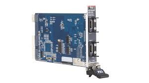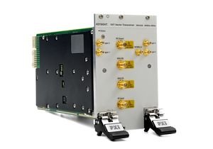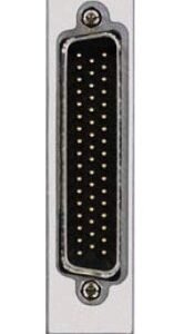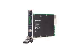

The National Instruments PXI-6534 is a 32-bit digital I/O interface module designed for high-performance pattern I/O, stimulus-response testing, and digital verification within PXI systems. It provides 32 individually configurable digital I/O lines compatible with 5V TTL/CMOS logic levels, with flexible port grouping for single-line, 8-bit, 16-bit, or 32-bit operations. The module delivers data transfer rates up to 80 MB/s for 32-bit transfers and supports pattern I/O at 20 MHz maximum frequency. Onboard 64 MB memory (two 32 MB banks) enables deterministic high-rate pattern generation and capture without host intervention. Each output line sources or sinks 24 mA, while input stages feature diode termination and 500 mV hysteresis for robust signal acquisition. The PXI-6534 integrates PLL circuitry for phase-locked synchronization with other PLL-equipped devices and supports triggering via the PXI trigger bus or RTSI bus for coordinated multi-instrument operation. Programmable pull-up and pull-down resistors on control and data lines allow customized power-on states. Change detection resolution is 150 ns, enabling precise edge capture and timing analysis. The module connects to external circuitry via a 68-pin SCSI-II connector and operates at 2.0 A from a +5 VDC supply. Industrial and research applications requiring precise timing, high throughput, and deterministic I/O operations benefit from the PXI-6534’s architecture and feature set.
Technical Specifications
• Channels: 32 digital I/O lines, individually configurable
• I/O Standard: 5V TTL/CMOS compatible
• Output Drive: 24 mA sink/source per line
• Input Levels: 0–0.8 V (low), 2–5 V (high)
• Input Hysteresis: 500 mV
• Maximum Transfer Rate: 80 MB/s (32-bit), 77.8 MB/s (with handshaking)
• Pattern I/O Rate: 20 MHz
• Change Detection: 150 ns resolution
• Onboard Memory: 64 MB (two 32 MB banks)
• Power Supply: 2.0 A at +5 VDC
• Connector: 68-pin SCSI-II (male)
– Key Features
• Port grouping supports single-line, 8-bit, 16-bit, or 32-bit pattern transfers
• PLL synchronization for deterministic timing with other PXI modules
• Configurable pull-up (2.2 kΩ control, 100 kΩ data) and pull-down resistors
• Start and stop triggering with PXI trigger bus and RTSI bus compatibility
• High-impedance power-on output state with selectable pull configurations
• Diode-terminated inputs for signal integrity at TTL levels
– Typical Applications
• Pattern-based stimulus and response testing
• Digital device verification and characterization
• Custom communication protocol implementation
• High-speed data acquisition and generation
• Synchronized multi-module test sequences
– Compatibility & Integration
The PXI-6534 integrates into any PXI chassis and synchronizes with other PLL-equipped instruments via onboard phase-lock circuitry. The module supports both PXI trigger bus and RTSI clock/trigger distribution for coordinated timing across test benches. Five-volt TTL/CMOS compatibility ensures straightforward interfacing with legacy and modern digital logic.