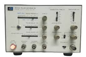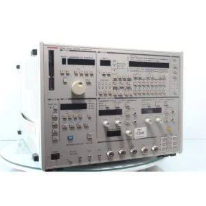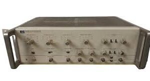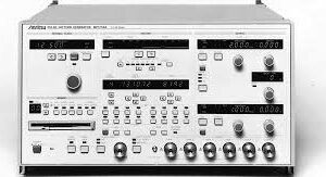

The Tektronix DG2040 is a data pattern generator engineered for high-speed digital testing and device characterization across frequencies from 0.1 Hz to 1100 MHz. It delivers dual-channel complementary outputs capable of 1.1 Gb/s data rates with pattern depths up to 256 K per channel, making it suitable for ASIC and FPGA verification, digital semiconductor evaluation, and system-level functional simulation.
Technical Specifications
Data Generation
• Data rate: Up to 1.1 Gb/s
• Pattern depth: 256 K/channel
• Output channels: 2 with complementary outputs
• Transition time (20–80%): <150 ps at 1 Vp-p, 10 MHz
• Sequence steps: Up to 4000
• Block repeats: 1 to 65,536 or infinite per line
Output Characteristics
• Output voltage (into 50 Ω): –0.875 V to +3.5 V (VOH); –1.125 V to +3.25 V (VOL)
• Voltage swing: 250 mVp-p to 5 Vp-p maximum
• Voltage resolution: 5 mV
• DC accuracy: ±3% of set value ± 50 mV
• Output impedance: 50 Ω
• Overshoot/undershoot: <5% at 1.5 Vp-p, 10 MHz
Timing and Jitter Control
• Output delay range: –1 ns to +2 ns
• Delay resolution: 10 ps
• Jitter adjustment: ±100 ps in 5 ps steps
• Clock period jitter (typical): <30 ps p-p at 1100 MHz
• CH0 period jitter (typical): 0.5 Vp-p
• Trigger impedance: 1 kΩ or 50 Ω selectable
• Maximum trigger input: ±10 V (1 kΩ); ±5 V (50 Ω)
• Minimum trigger pulse width: ≥10 ns
– Key Features
• Flexible sequence control with jump, event, and nested loops
• Variable output delay and edge timing for jitter simulation
• External modulation capability for continuously variable jitter
• SMA connectors at front panel for CH0, CH1, and clock; rear panel for auxiliary inputs
– Typical Applications
• ASIC and FPGA design verification
• Digital semiconductor characterization
• High-speed logic circuit testing
• Serial data stream simulation with controllable edge timing
– Compatibility & Integration
The DG2040 interfaces via front-panel SMA outputs and BNC trigger input, with rear-panel clock reference and event inputs for system integration.