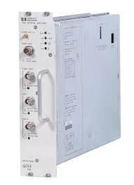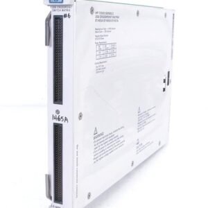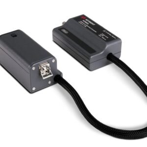


The Agilent J1421A is a register-based VXI clock source module designed for high-speed optical testing environments. This C-size, two-slot module generates precise clock outputs at 10 Gb/s or 2.5 Gb/s with adjustable frequency offset to ±20 ppm, synchronizing transmit and receive operations across test systems. Direct register access enables control and status monitoring without external dependencies.
Technical Specifications
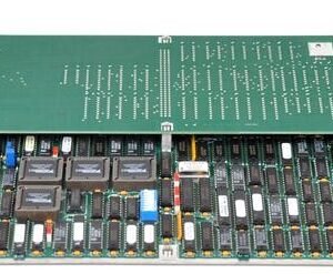
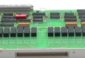
• Module Type: VXI (VME eXtensions for Instrumentation), C-size, two-slot form factor
• Clock Generation Output: 10 Gb/s, 2.5 Gb/s
• Frequency Offset: ±20 ppm
• External Reference Source Input: 156 MHz, 622 MHz, 2.5 GHz
• External Clock Input: 10 GHz, 2.5 GHz
• Operation Mode: Register-based with direct register access
– Key Features
• Dual clock output rates support both high-speed and standard-rate optical applications
• Frequency offset adjustment enables fine-tuning for timing compensation and synchronization verification
• Multiple external reference inputs (156 MHz, 622 MHz, 2.5 GHz) accommodate diverse master clock architectures
• High-frequency clock inputs (10 GHz, 2.5 GHz) allow direct slaving to external timing sources
• Synchronization capability with the Agilent J1420B Receiver module via 156 MHz clock recovery
• Register-based control simplifies integration into automated test frameworks
– Typical Applications
• Multi-rate optical transceiver testing at 10 Gb/s and 2.5 Gb/s
• Transmit/receive module synchronization in high-speed test systems
• Frequency offset and timing margin validation
• Master clock distribution in VXI-based optical test benches
– Compatibility & Integration
The J1421A integrates into standard VXI chassis environments and pairs directly with the J1420B Receiver module for clock recovery-based synchronization. External timing sources connect via dedicated clock input/output connectors supporting the specified frequency ranges.