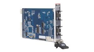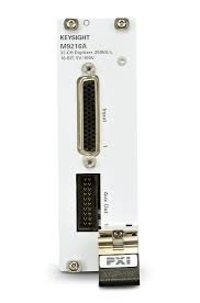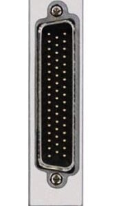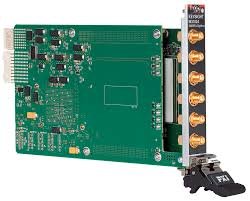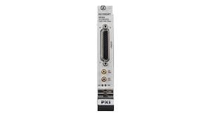

The National Instruments PXI-6543 is a high-speed digital I/O module for PXI systems delivering 32 individually configurable bidirectional channels operating at data rates up to 50 MHz. The module supports programmable logic levels (5.0 V, 3.3 V, 2.5 V, 1.8 V) for multi-family logic interfacing, with each line capable of sourcing or sinking up to 24 mA. Channel configuration is flexible—organize all 32 lines into four 8-bit ports or configure individually. The onboard Synchronization and Memory Core (SMC) technology enables complex waveform sequences and single-shot or continuous waveform generation, with onboard memory available in 1 Mbit, 8 Mbit, or 64 Mbit configurations per channel. Clock options include an internal voltage-controlled crystal oscillator (VCXO) with divider, external clock input via SMB connector, or synchronization with the PXI backplane clock (PXI_STAR). TTL/CMOS-compatible triggering supports digital pattern detection, rising/falling edge triggers with 10 ns minimum pulse width recognition, and full PXI trigger bus compatibility. The module interfaces via a 68-pin male SCSI-II I/O connector, with front-panel SMB and DDC connectors for clock and strobe inputs. Input voltage range extends from -0.3 V to 5 V absolute maximum. Timing specifications apply at the DDC connector and high-speed DIO accessory terminals.
Technical Specifications
• 32 bidirectional channels, individually configurable or grouped into four 8-bit ports
• Maximum data rate: up to 50 MHz
• Output current drive: 24 mA source/sink per line
• Input voltage range: -0.3 V to 5 V (absolute maximum)
• Programmable logic levels: 5.0 V, 3.3 V, 2.5 V, 1.8 V
• Sample clock duty cycle: 25–75% (< 50 MHz), 40–60% (≥ 50 MHz)
• Onboard memory: 1 Mbit, 8 Mbit, or 64 Mbit per channel configurations
• I/O connector: 68-pin male SCSI-II
• Clock inputs: internal VCXO with divider, external CLK IN (SMB), PXI_STAR backplane
• Trigger input: STROBE via DDC connector (acquisition only)
– Key Features
• Synchronization and Memory Core (SMC) technology for waveform generation and instruction management
• Single or complex sequence waveform generation (waveforms must be integer multiple of 2 samples)
• TTL/CMOS digital pattern and edge triggering (5 V trigger level)
• Pattern match/mismatch detection on user-defined data lines
• Edge trigger minimum pulse width: 10 ns
• PXI star trigger and trigger bus compatibility
• Multi-voltage logic family support in a single module
– Typical Applications
• Digital test and control in PXI modular instrumentation platforms
• Multi-protocol digital I/O stimulus and acquisition
• Waveform generation with complex sequencing
• High-speed digital pattern matching and triggering
– Compatibility & Integration
The PXI-6543 integrates with PXI systems via the backplane clock (PXI_STAR) and trigger infrastructure. External timing sources connect via front-panel SMB and DDC connectors. Digital I/O termination and accessory interfacing use standard 68-pin SCSI-II connectivity.