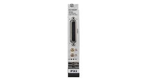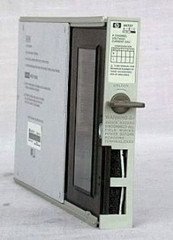

The NI PXI-7833R is a reconfigurable I/O (RIO) multifunction module engineered for high-performance measurement and control applications requiring custom timing, triggering, and onboard signal processing. Built around a Virtex-II 3M gate FPGA (XC2V3000), it delivers 28,672 flip-flops, 96 embedded 18×18 multipliers, and 1728 Kbits of block RAM for complex digital signal conditioning and real-time algorithms. The module integrates 8 analog input channels (16-bit, 200 kS/s, ±10 V), 8 analog output channels (16-bit, 1 MS/s, ±10 V), and 96 bidirectional digital I/O lines operating at up to 40 MHz. All I/O is programmable via LabVIEW and the LabVIEW FPGA Module, enabling rapid prototyping within the PXI ecosystem.
Technical Specifications
FPGA & Logic:
• Virtex-II 3M gate (XC2V3000) with 28,672 flip-flops
• 96 embedded 18×18 multipliers
• 1728 Kbits embedded block RAM
• Programmable via PXI trigger lines (8 lines) and RTSI bus access
Analog Input:
• 8 channels, 16-bit resolution, 200 kS/s per channel
• ±10 V input range, DC coupling
• Single-ended or differential mode (differential uses two AI lines per channel)
Analog Output:
• 8 channels, 16-bit resolution, 1 MS/s update rate
• ±10 V output range, 1.25 Ω impedance, ±2.5 mA drive
• DC coupling, short-circuit protected, user-configurable power-on state
Digital I/O:
• 96 bidirectional lines configurable as inputs, outputs, counters, or custom logic
• 40 MHz custom logic rates; 3.3 V and 5 V TTL compatible
• ±4.0 mA source/sink, 25 ns minimum input pulse width, 12.5 ns output
• Input protection: −0.5 to 7.0 V; output short-circuit protection (up to 8 lines)
Timing & Synchronization:
• FPGA device clock phase-lockable to PXI chassis 10 MHz reference
• PXI Star Trigger support for inter-slot communication
• Single-cycle timed loop support for digital I/O
Power & Physical:
• 727 mA @ 3.3 V ± 5%; 250 mA available per I/O connector pin @ 4.50–5.25 V
• Dimensions: 6.3 × 3.9 in.; 1 lb
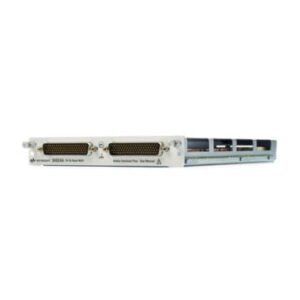
• SCB-68 shielded connector block
– Key Features
• Flexible FPGA fabric for custom DSP, timing, and control logic
• Phase-locked FPGA clock synchronizes with PXI chassis and RTSI infrastructure
• Programmable digital I/O states and protection thresholds
• Mixed-signal capability: simultaneous analog and digital acquisition/generation
• Minimum 5 ns sampling period for digital operations
– Typical Applications
• Real-time signal conditioning and filtering
• Custom triggering and timing synchronization
• Parallel analog and digital measurement acquisition
• Closed-loop control with hardware-timed feedback
• Multi-slot PXI system integration with synchronized sampling
– Compatibility & Integration
Plugs into any PXI slot; integrates with LabVIEW FPGA Module for graphical HDL design. Accesses PXI trigger lines, star trigger (slot 2), and RTSI bus for chassis-wide synchronization. Compatible with SCB-68 accessory connector blocks for custom signal routing.